This is followup to my post about building a low cost wifi camera. I mentioned that the Esparducam board is well suited for ESP8266 development in general and here is why. In addition to the Esparducam board I also designed a number of addon boards. The boards are very small (21×26 mm) meaning you can fit two of them into a standard 50×50 mm PCB you can get produced for very little money. If you want to try a new component or connector and perhaps a newly designed footprint, make a “boardlet” and try it on the Esparducam.
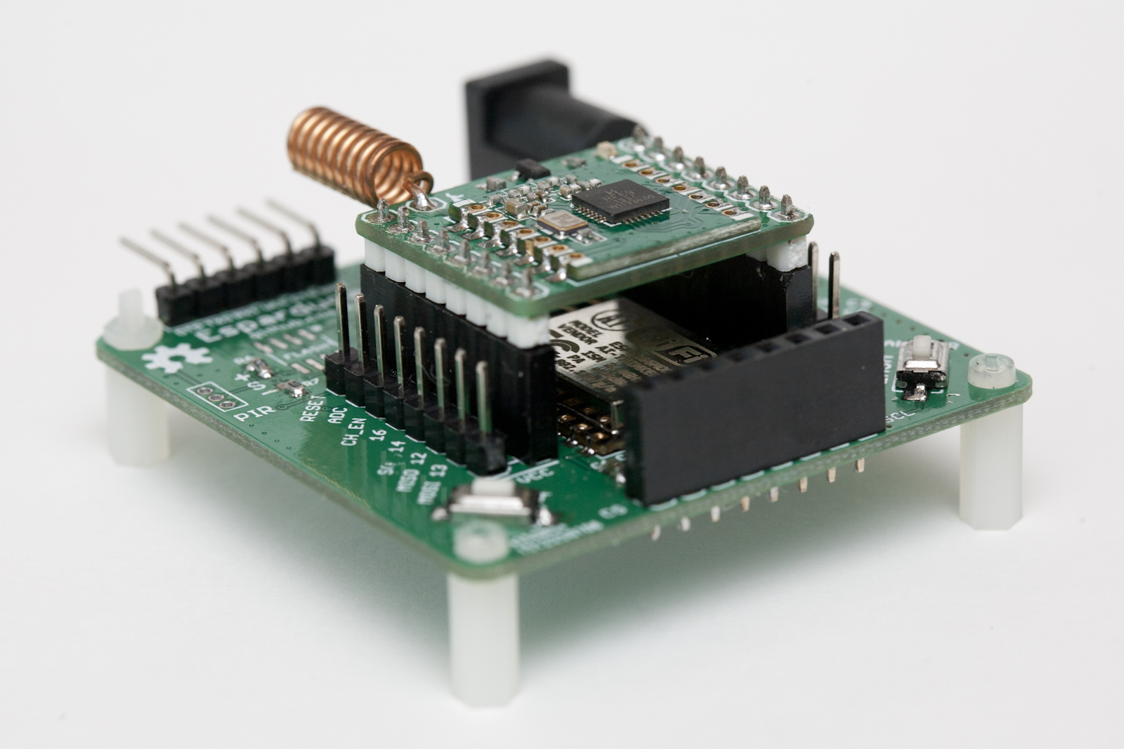
The “ISM boardlet” mounts an RFM96C for building a low cost ISM to Wifi gateway. The board has an optional LED (driven by a mosfet) for link indication. I ported André Heßling’s RFM69-STM32 driver for this board and even though I have not had the time to test that much, basic transmission works.
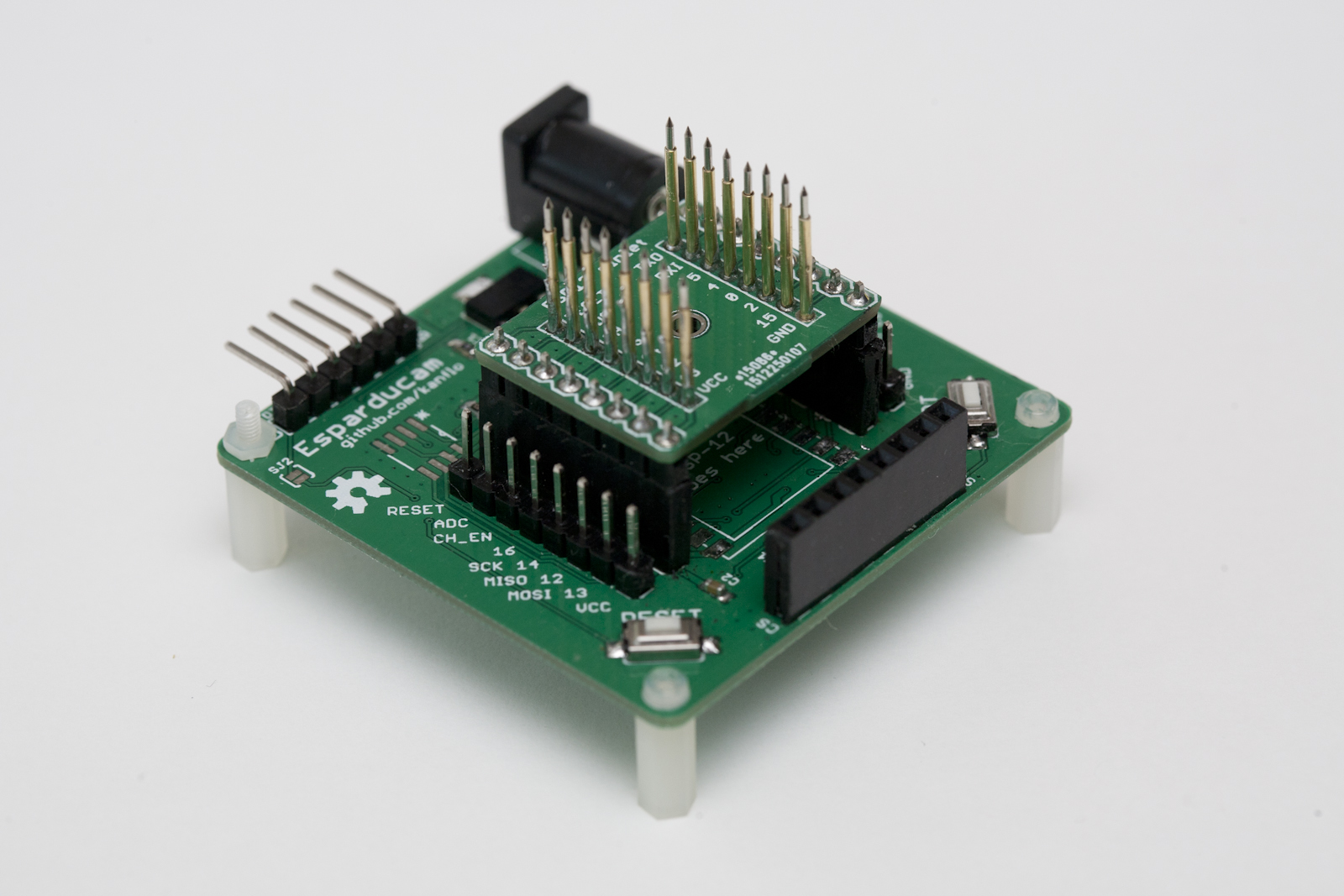
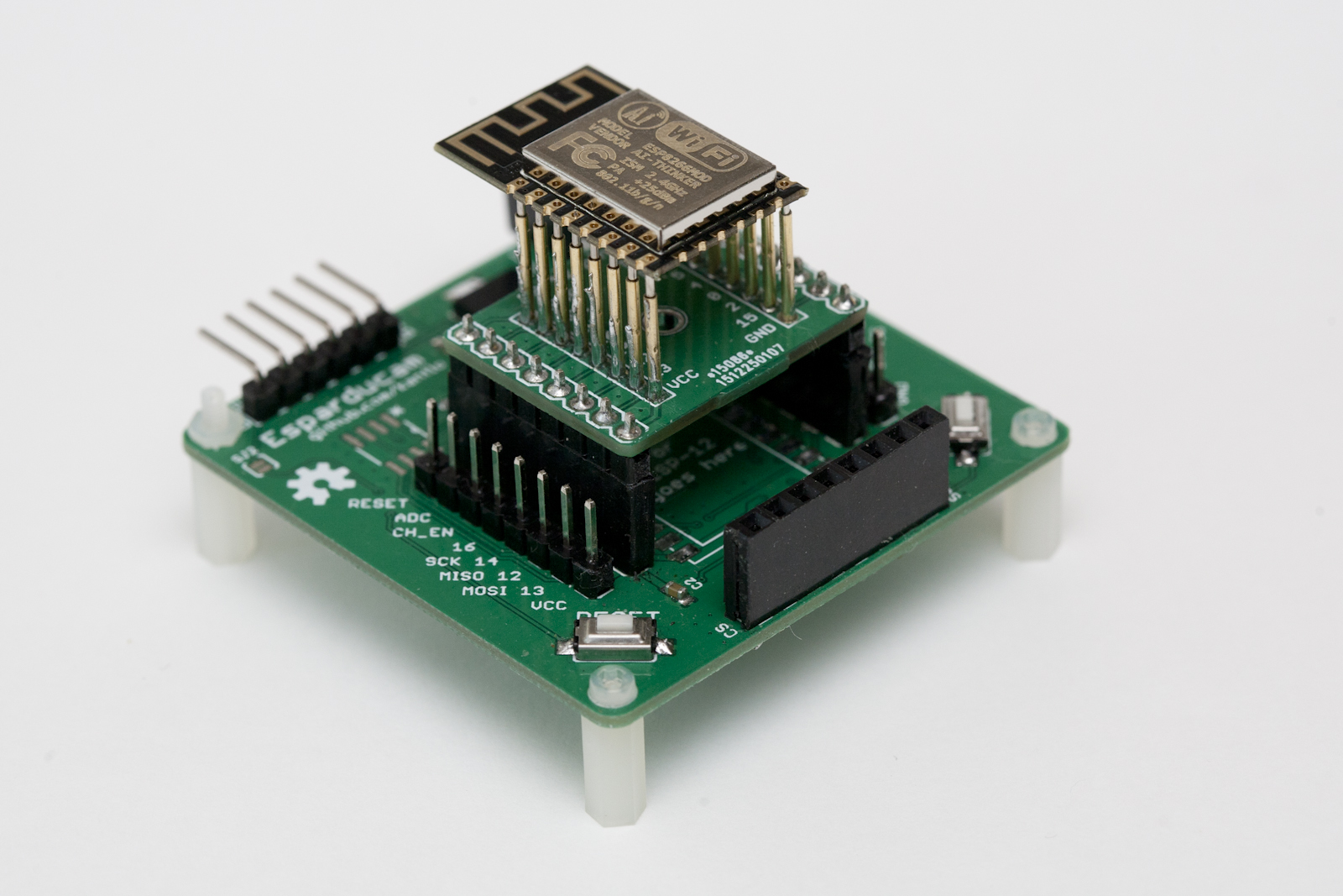
The next board, the esp-pinlet, serves as a test bench for ESP12 family modules. After soldering an ESP12e module to an Esparducam board I noticed it would not connect to my Wifi network. For the price of ESP8266 modules, I cannot complain about broken modules but I want to make sure the modules I mount on my boards actually work before soldering. So how do we test ESP12 modules without soldering? Pogo pins! The pinlet board has 1.02mm (40 mil) holes for pogo pins that allows for an ESP12 module to be firmly pressed against the pins while flashed and tested. You can find these on eBay.
Schematics on Github.
Update on April 27th
Th pogo pins I used initially where not that good as the needle like shape made them get stuck in some of the ESP12 modules. A much better alternative is the P75-E2 [eBay] type of pin (still 1.02mm / 40mil):
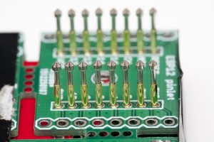
If you plan on building a pinlet board, make use of the fact that you get ~10 in each order to help with alignment.
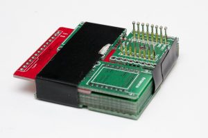
The stack here (top to bottom) is the board having the pins mounted, a spacer board (the red one), five pinlet boards for alignment and at the bottom one board flipped upside down to keep the pins from sliding downwards. The package is fixed with tape and ready for solder.
Pingback: Building a low cost wifi camera – Johan Kanflo
Pingback: Truly Versatile ESP8266 WiFi Webcam Platform | Hackaday
Pogo pins! Brilliant, thanks!
Hey,
Do you have the gerber files for the ESP Pinlet or is it already on dirty pcb? I’d like to put one together.
Alternately, which PCB making software/version did you make this in? I can’t get it to open in Kicad 4.0.1 on Windows.
Thanks,
I used Eagle (should have used Kicad, I know…). I just added the pinlet gerbers to Github. They look ok on circuitpeople.com but it’s not the gerbers I produced from (those contain other designs that I have not finalized yet).
I’m looking to get some of these boards made up myself to program some of my esp-12e’s. I’m not really familiar with board design, but the GND pogo pin doesn’t show a path to the GND pin. Is that on purpose? I’m sorry if it’s an obvious answer…
Nice, please send pictures 🙂 One fundamental aspect of board design is the ground plane (Wikipedia has a nice article). If you look at the png of the board (https://github.com/kanflo/esparducam/blob/master/hardware/esp-pinlet/esp-pinlet.png) the green GND pads are connected to the red ground plane (and the blue bottom one). Learning basic board design is great fun. I can recommend building someone else’s board, taking the Sparkfun/Adafruit Eagle tutorials (or finding Kicad equivalents) and finish with a design of your own.
Oh, when ordering pogo pins make sure you order 1.02 mm diameter pins. I tried the P75-B1 which is rather pointy. I have some P75-E2 in transit that I will try. When soldering you can use an extra pinlet board to help with alignment.
I’ll look into the tutorials! I figured there was an obvious answer but just wanted to ask and confirm, thanks for being kind with your response. I actually have some P75-B1’s in my parts bin already 🙂
It’s obvious on this side of the board design learning curve. You will have much fun getting here. 🙂
LAst question… for now haha…I forgot to ask, do I need to populate C1, C2 and C3 as per your schematic for the esp-12e?
Those are decoupling capacitors (https://en.m.wikipedia.org/wiki/Decoupling_capacitor) and are needed for stabilising the power supply for the IC. You might do without them but chances are weird things start to happen when there is a dip on your VCC rail.
Hi Johan,
These look awesome!! I’m particularly interested and excited about your ESP8266 and RFM69 board. What code did you use to program the ESP8266 board to communicate with the RFM69 transmitter? Any help is much appreciated!!
Thanks! I made a port of a driver for the STM32. I will put it on GitHub this weekend.
Hi Johan,
Thanks! Were you able to add it to your git? I took a quick look, but wasn’t able to find it here: https://github.com/kanflo/
Thank you!
Sorry, it slipped my mind. You can find it at here now.
Hi johan,
could you explain the use of RFM69C with esp8266. What does it do?
Hi Amol. The RFM69C is for building a inexpensive ISM radio gateway. I currently have a Raspberry Pi with the BranlyPi board but plan to replace that with an ESP8266/RFM69C combo.